The scariest thing about static isn't that it destroys a chip on the spot — that, at least, is easy to catch. The real trouble is when it wounds a chip internally yet still lets it power up and pass test, until the chip goes into a light string, sells to a customer, glows for a few months, and then fails without warning. This invisible harm is called latent damage. Defending against it relies not on any single piece of equipment, but on a whole system spanning people, equipment, and packaging. This article is about how to build static protection on an LED line.
- Why static is an “invisible” killer
- First define sensitivity: HBM and CDM
- Grounding is the foundation, but grounding can’t save an insulator
- From single-point equipment to the EPA: making protection a space
- Auditing and discipline: a system isn’t effective just because it’s installed
- PowerMOS: building interference immunity into the chip to lower overall exposure
- References and standards
- FAQ
The scariest thing about static isn’t that it destroys a chip on the spot — that, at least, is easy to catch.
The real trouble is when it wounds a chip internally yet still lets it power up and pass factory test, until the chip goes into a light string, sells to a customer, glows for a few months, and then fails without warning. This invisible harm has a name: latent damage. Defending against it relies not on any single piece of equipment, but on a whole system spanning people, equipment, and packaging. This article is about how to build static protection on an LED line.
Why static is an “invisible” killer
When a person walks across a carpet and a spark jumps from a fingertip to a doorknob, the voltage can reach several thousand volts. The static a person can feel is usually already above three thousand volts; but the static that can wound a modern chip may take only one or two hundred volts — far below the threshold a human body can perceive.
That is the first layer of the problem: you can’t feel the harm as it happens. The operator never gets a shock, yet the chip is already damaged.
The second layer is worse. Static harm to a chip comes in two kinds: one is catastrophic failure, where the chip burns out on the spot, functional test catches it immediately, and it is stopped inside the line; the other is latent damage, where static merely weakens the device’s microscopic internal structure — the chip still works and passes test, but its reliability has quietly been discounted. It may fail weeks to months after power-up — by which time the product has long since shipped, and the cost of interception jumps from a few dollars on the line to the enormous price of recalls, repairs, and reputation.
Precisely because it is invisible, untestable, and delayed, static is the invisible killer on the line that must be defended by discipline rather than luck.
First define sensitivity: HBM and CDM
To manage risk, you first have to quantify how fragile a device is. The industry uses two discharge models to describe a chip’s static sensitivity:
- Human Body Model (HBM): simulates the discharge when a charged human body touches a device, representing the most common “person touches chip” scenario.
- Charged Device Model (CDM): simulates the instantaneous discharge when a device that is itself charged touches a grounded object, common during automated pick-and-place.
The international standard ANSI/ESD S20.20 uses these two models to define control thresholds: devices sensitive to discharge at HBM 100V and CDM 200V and above should all be brought into the static control program[1]. In other words, the vast majority of semiconductor devices — LED pixel-control chips among them — fall within the range that needs protection. Only by knowing what you are protecting against, and to what degree, can you design the matching measures.
Grounding is the foundation, but grounding can’t save an insulator
The core logic of static protection is a single sentence: hold everything at the same potential. No potential difference, no discharge.
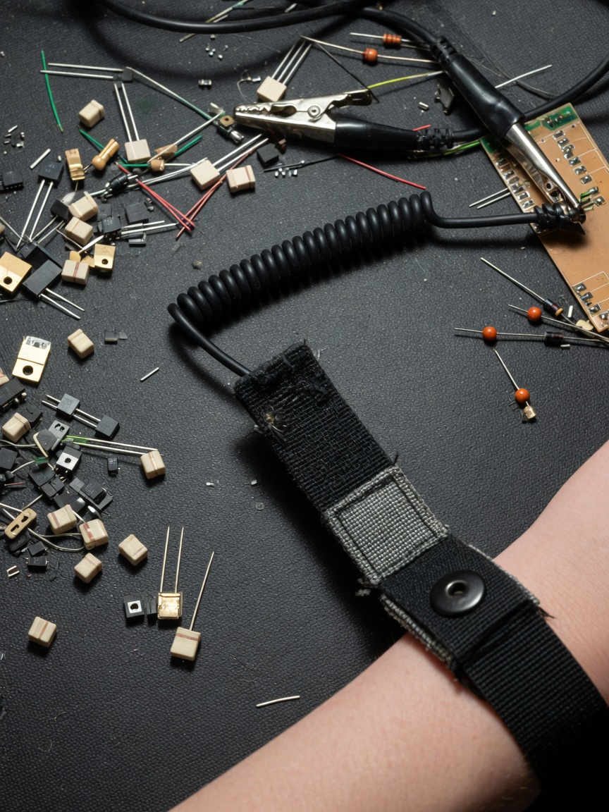
The first step to achieving this is grounding. Operators wear grounding wrist straps to continuously drain static from their bodies; workbenches are lined with anti-static bench mats connected to a common ground point; floors are laid with anti-static floor mats and personnel wear anti-static footwear. This “person–bench–floor” grounding network holds the world of conductors at the same potential.
But grounding has an inherent limit: it only works on conductors. The charge accumulated on insulators — plastic trays, tape, bubble bags, packaging film — cannot be released along a ground path, because the charge simply won’t flow. That is where an ioniser comes in: it produces positive and negative ions to actively neutralize the charge on an insulator’s surface. On the line, any non-conductor that cannot be grounded yet sits near sensitive devices is within the ioniser’s remit. Grounding and ionic neutralization — one for conductors, one for insulators — together form the complete first line of defense.
From single-point equipment to the EPA: making protection a space
With grounding and ionic neutralization in place, one thing is still missing — a framework that integrates them; otherwise the equipment works in isolation and gaps are inevitable. That framework is the EPA (ESD Protected Area).
An EPA is a work area where all objects are held at the same potential and static is controlled[2]. It turns scattered equipment into a controlled space with boundaries and rules:
- Before entering the EPA, personnel must wear and verify their grounding wrist strap or anti-static footwear — measured to confirm continuity, not merely put on.
- Benches, mats, equipment, and tools inside the area are all connected to a common ground point.
- Non-conductors are neutralized by ionisers, or moved out of the sensitive area entirely.
- The boundary is clearly marked, and unprotected sensitive devices may only be unpacked and handled inside the EPA.
The key is the “moment of unpacking”: static-sensitive devices should be transported only inside the EPA and in anti-static (ESD) packaging, protected by shielding or dissipative bags whenever they leave the controlled environment. Controlled inside the area, protected by packaging outside it — the two hand off so the device never leaves protection from incoming inspection through to assembly.
Auditing and discipline: a system isn’t effective just because it’s installed
The most easily overlooked point is this: static protection is not a one-time purchase but an ongoing discipline. Wrist straps come loose, mats wear out, ground wires break, and an ioniser’s ion balance drifts. Equipment is at its most effective the day it is installed; from there it only degrades.
That is why the spirit of ANSI/ESD S20.20 has never been “buy all the equipment,” but to require building an auditable control program: regularly measuring wrist-strap and grounding continuity, periodically verifying ionisers, recording and tracking anomalies, and training personnel[1]. The strength of a protection system depends on whether its weakest link keeps getting caught.
PowerMOS: building interference immunity into the chip to lower overall exposure
A line’s static protection guards the environment side; the device’s own tolerance on the design side decides how much consequence the same environmental risk produces.
PowerMOS pixel-control chips build in surge- and static-protection considerations at the design stage, and adopt a single-point-failure-non-propagating architecture — even if an individual bead is damaged, it will not spread along the whole string, keeping a single-point mishap confined to a single point. Combined with replaceable-bead repair design, single-device handling in downstream assembly and field maintenance becomes more controllable. Flagship parts such as the P9864/P9866 (RGB three-channel), P9865/P9873 (RGBW four-channel), and P9871/P9874/P9875 (copper-wire series) all carry forward this interference-immune, fault-tolerant design approach. See the Product Center for full part numbers, and for line-integration questions contact sales-02@powermos.com.
Further reading: for overall reliability against surge and EMC, see The EMC, ESD, and Surge Reliability Engineering of LEDs; for factory compliance, see The Safety Certification System of LEDs.
References and standards
- ANSI/ESD S20.20, Protection of Electrical and Electronic Parts, Assemblies and Equipment (Excluding Electrically Initiated Explosive Devices). EOS/ESD Association, Inc.
- IEC 61340-5-1, Electrostatics — Part 5-1: Protection of electronic devices from electrostatic phenomena — General requirements. International Electrotechnical Commission (IEC).
This article is an educational overview of static protection. The names of the cited standards can be verified in the EOS/ESD Association and IEC official catalogs. PowerMOS pixel-control chips use a proprietary carrier protocol optimized for LED pixel control.
FAQ
What is ESD latent damage?
Static harm to a chip comes in two kinds. One is catastrophic failure — the chip burns out on the spot and functional test catches it. The other is latent damage, where static merely weakens the device's internal structure; the chip still works and passes factory test, but its reliability has quietly been discounted. It may fail weeks to months after power-up, by which time the product has long since reached the customer, and the repair and reputation cost far exceeds catching it on the line. Latent damage is exactly the invisible killer that static protection must prioritize.
What is the core of the ANSI/ESD S20.20 standard?
ANSI/ESD S20.20 is the management and technical standard for an electrostatic discharge control program. Its core is not to dictate which equipment to buy, but to require building a complete control program covering grounding, personnel equipment, packaging, and auditing. The standard uses the Human Body Model (HBM) and the Charged Device Model (CDM) to define sensitivity thresholds — devices sensitive at HBM 100V and CDM 200V and above should be brought under control. It elevates static protection from single-point equipment to a systematic discipline.
What is an EPA static-protected area?
An EPA (ESD Protected Area) is a work area where all objects are held at the same potential and static is controlled. Before entering an EPA, personnel wear grounded wrist straps or anti-static footwear; benches and floor mats connect to a common ground point; and non-conductors are neutralized by ionisers. The EPA boundary is clearly marked, and unprotected devices may only be unpacked and handled inside it. It is the key concept that integrates scattered protective equipment into one controlled space.
When is an ioniser actually needed?
Grounding can only drain static from conductors; it does nothing for insulators like plastic, tape, and packaging — the charge they accumulate cannot be released through a ground path. That is where an ioniser comes in: it produces positive and negative ions to neutralize the charge on an insulator's surface. On the line, any non-conductor that cannot be grounded yet sits near sensitive devices is within the ioniser's remit. It covers the gap the grounding system cannot reach.
How do PowerMOS pixel-control chips address the line's static risk?
PowerMOS pixel-control chips build in surge- and static-protection considerations at the design stage, and adopt a single-point-failure-non-propagating architecture — even if an individual bead is damaged, it will not spread along the string. Combined with replaceable-bead repair design, this makes single-device handling in downstream assembly and field maintenance more controllable. These design choices lower the overall exposure of the line and the field to static damage. See the Product Center for full part numbers.
Upgrading your string lights to full pixel control?
Power MOS Electronics delivers the complete stack — driver ICs, addressing equipment, controllers and apps. Tell us about your product and our engineering team will spec it with you.
Contact PowerMOS Browse products